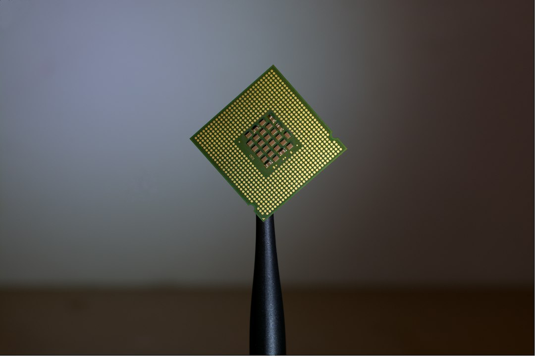
Photo by Brian Kostiuk on Unsplash
Write Combining Buffers: Merging Sequential CPU Writes
Modern CPUs include a specialized piece of hardware called write combining buffers (WCBs) that batch multiple sequential memory writes into fewer, larger transactions. This optimization reduces bus traffic and improves performance for specific workloads, but it comes with ordering guarantees that differ from normal cacheable memory.
How Write Combining Works
When a CPU writes to memory, it typically goes through the cache hierarchy. For cacheable memory, writes update the L1 cache, eventually making their way to main memory through write-back or write-through policies. Write combining takes a different approach for uncached memory regions.
A write combining buffer holds multiple pending writes to adjacent memory addresses. Instead of issuing each write separately across the memory bus, the CPU merges them into a single larger transaction. A typical implementation uses 4 to 10 buffers, each holding 64 bytes worth of writes. When a buffer fills up, times out, or encounters a memory fence instruction, the CPU flushes the combined write to memory.
The key insight is that many sequential writes—like filling a frame buffer or writing to memory-mapped I/O—benefit from batching. A loop writing individual bytes to consecutive addresses can be coalesced into a single 64-byte burst transaction, dramatically reducing the overhead of initiating separate bus cycles.
Memory Type and Ordering
Write combining is explicitly configured through page table attributes or memory type range registers (MTRRs). Operating systems mark specific physical address ranges—typically device memory for graphics cards or network adapters—as write-combining rather than cacheable.
Unlike cacheable memory, write combining provides weaker ordering guarantees. Writes to WC memory can be reordered, merged, or delayed. The CPU makes no guarantee about when buffered writes will become visible to other observers. This relaxed model enables the performance gains but requires explicit synchronization when ordering matters.
A memory fence instruction (like sfence on x86) forces all pending WC writes to flush. Without a fence, writes might sit in buffers indefinitely or emerge in unexpected orders. Code that writes to device memory and then expects the device to observe those writes must include an appropriate barrier.
Graphics and Device Memory
The primary use case for write combining is graphics memory. When a CPU writes pixel data to a GPU’s frame buffer, it’s writing to uncached, memory-mapped device memory. Without write combining, each pixel write would trigger a separate bus transaction, saturating the PCIe link with tiny transfers.
With write combining enabled, the CPU batches those writes. A loop filling a scanline can accumulate dozens of pixel writes in a buffer before flushing them as a single burst. This reduces PCIe overhead and leaves more bandwidth for GPU-to-CPU reads or other DMA traffic.
Network adapter ring buffers, DMA descriptor lists, and other memory-mapped hardware regions also benefit from write combining. Any scenario where software writes sequential data to device memory is a candidate.
Performance Characteristics
Write combining delivers substantial speedups for sequential write patterns but can hurt performance for scattered writes. If a program writes to widely separated addresses, it thrashes the limited number of WC buffers, causing frequent flushes and defeating the batching mechanism.
Alignment matters as well. WC buffers operate on cache-line-sized chunks, typically 64 bytes. Writes that cross alignment boundaries may require multiple buffer entries or trigger premature flushes. Performance-sensitive code often pads structures or aligns allocations to cache line boundaries to maximize WC efficiency.
Read-modify-write operations don’t work well with write combining. Because WC memory is uncached, reading from a WC region forces the CPU to fetch from the device, bypassing any buffered writes. The typical pattern is write-only: fill a buffer with data and let the device read it.
Interaction with Modern Hardware
On contemporary systems, write combining interacts with other memory subsystem features. Non-temporal store instructions (like movnti or vmovntdq on x86) hint that data won’t be reused soon, bypassing the cache and potentially using WC buffers even for normal memory.
PCIe relaxed ordering is another related mechanism. PCIe transactions can be marked as allowing reordering at the interconnect level, complementing the CPU-side reordering that write combining enables. Together, these techniques optimize the full path from CPU to device.
Some architectures implement posted writes or store buffers that serve a similar purpose for regular memory, but write combining is distinct in its application to uncached regions and its explicit configuration through memory types.
Practical Considerations
Developers rarely interact with write combining directly in application code. The operating system configures memory types when mapping device memory, and driver code handles the details. Graphics APIs and DMA libraries abstract the complexity.
When it does surface, the key rule is simple: treat WC memory as write-only, write sequentially when possible, and fence before expecting visibility. Profiling tools that monitor PCIe utilization or memory bus traffic can reveal whether write combining is working as intended—you should see larger, less frequent transactions rather than a stream of small writes.
Write combining is a hardware optimization that remains relevant as device bandwidth grows. Even with PCIe 5.0 and beyond, reducing transaction overhead and bus contention matters. The technique represents a broader principle in systems design: batching and coalescing small operations into larger ones often unlocks performance that individual optimizations cannot achieve.